Hardware Design
Our CAD environment streamlines the design flow by seamlessly integrating design capture, synthesis, simulation and implementation. Whilst there are no substitutes for talent and intuition, powerful design tools allow new ideas to be evaluated rapidly.
Schematic Capture

Circuit schematics are the starting point for board level design. A rigorous checking procedure ensures that the electrical, physical and ordering information associated with the devices in our component libraries is complete and correct. Completed schematics are then subjected to internal review and if appropriate a client review prior to PCB layout.
HDL and Synthesis
The power and portability of hardware description languages such as VHDL and Verilog has made them the design methodology of choice for ASIC, FPGA and large CPLD designs. A library of tested functions described by HDL source code can be integrated into new designs to reduce design time. Our CAD tools also provide support for test bench development, source code simulation and post synthesis (gate level) simulation.

Simulation

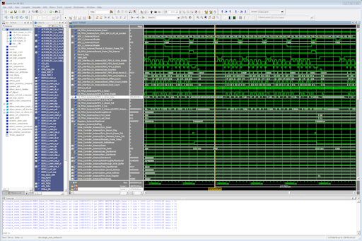
Whilst the design capture programs can detect some connectivity errors, design verification really starts with the simulator. Functional simulation confirms that the HDL source is logically correct before synthesis. Whilst it is possible to re-simulate using the signal delay information that is generated during compilation in order to determine whether the design will operate at the chosen frequencies; most designs are large enough to make this a very slow operation. The normal approach now is to set timing constraints and to use the compiler tools to check for timing closure. Debugging of the compiled design can then be achieved using the FPGA manufacturer's signal tapping tools which use spare logic and RAM inside the FPGA to implement an on-chip logic analyser. A Spice based analogue circuit simulator can be used standalone or coupled to the digital simulator to support mixed mode system development.
PCB Layout and Routing
Correct PCB layout is critical to achieving signal integrity, high operating frequencies and reducing emitted radiation. Minimising track lengths reduces signal cross talk and reflection so PCB layout is guided or completed by the same person as did the electronic design. This level of circuit insight can achieve optimal component placement and properly handles potential problem areas such as high frequency digital transmission, sensitive analogue circuits, DC-DC converters and split power planes in order to minimise crosstalk and EMC issues. A choice of two state of the art autorouters is available to route the less critical board areas, configurable design rules allow suitable routing strategies to be applied to each board, or area within a board. Post route information can be passed to a signal integrity and EMC analysis package which can help in the selection of appropriate termination and highlight where routing or screening should be improved.

Procurement, Assembly and Test

Sourcing the components on a bill of materials takes a surprising amount of time, with long lead times becoming more common, finding product 'on the shelf' can be a chore. Large minimum order quantities can also be a problem at the prototype stage. Design Interface has built relationships with many component manufacturers and distributors which often allows us to get those elusive components quickly.
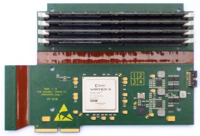
Small batches of boards are quickly built in-house, all component packages including BGA can be mounted. Rework equipment is available should changes be necessary. Our modular device programmer supports the vast majority of programmable components and package variations, although in-system programming is supported where possible. When larger production batches warrant it, we can introduce you to electronics assembly companies who are able to produce working boards or systems in large numbers.
Implementing systems using high clock rates and wide system busses requires that we employ high-end test equipment for analysis and signal integrity testing. EMC pre-compliance testing can be completed in-house.